Multilayer PCB Manufacturing up to 38 layers
Rigid Circuit Board Manufacturer & Assembly – One stop service PCB rigid Circuit Board is an important electronic component, support for electronic components, and a carrier for electrical connection of electronic components. Read on to learn more about multilayer PCBs, their uses and advantages in the world of modern electronics.
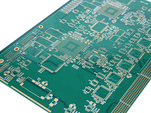
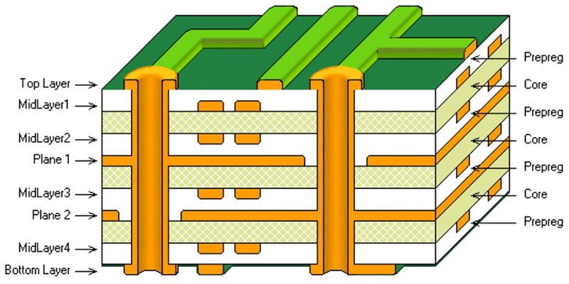
A Multilayer Printed Circuit Board, or Multilayer PCB, is a complex circuit board composed of multiple layers of conductive material and insulating material (usually fiberglass and epoxy resin) sandwiched together. Multilayer PCB or multilayer printed circuit boards are circuit boards composed of two or more conductive layers (copper layers). The copper layer is pressed together by the resin layer (prepreg). Each layer has a conductive path or copper trace, and each layer is connected to one another through pads and vias, which act as electrical conduits. This construction allows for more complex and dense circuitry to be designed, with greater functionality and reliability compared to single- or double-sided PCBs. Multilayer PCBs are commonly used in electronic devices such as computers, smartphones, and advanced medical equipment.

What is Multilayer Printed Circuit Board?
A Multilayer Printed Circuit Board (PCB) is a type of PCB that consists of several layers of conductive material and insulating material sandwiched together. The board is made by laminating together multiple thin layers of fiberglass or other insulating materials with copper foil.
An integrated circuit is placed on the board, and the copper traces connected to the circuit are etched onto the inner layers of the board. The inner layers are then sandwiched together with the outer layers, forming a multilayer structure.
Multilayer PCBs are used in high-end electronic products, such as advanced computers and mobile phones, where a high degree of density is required, and the manufacturing process is complex. They provide many benefits, including reduced size, increased reliability, and improved performance.
Multilayer PCBs are cost-effective because they reduce the total number of components needed and improve product reliability, thus reducing the need for frequent repair services or replacement. The design flexibility of these boards also allows for more efficient use of space and improved signal routing, which aids in the performance of the product.

So what’s Multilayer PCB Benefits / Advantages?
1. Increased Design Flexibility: Multilayer PCBs allow for more design flexibility and greater circuit density. With multiple layers, engineers have more space to incorporate more components and features, such as impedance control, shielding, and power planes, within the same board area.
2. Increased Reliability: Multilayer PCBs are more reliable than single sided PCBs, as they are less prone to issues such as signal interference, voltage drops, and thermal stress. This is because they have a higher number of conductive layers, which allows for better shielding and more stable power distribution.
3. Higher Component Density: Multilayer PCBs can accommodate a higher density of components in a smaller space while preventing signal interference. This results in a more compact and efficient design, saving manufacturers money on materials and production.
4. Improved Signal Integrity: With a multilayer construction, PCBs can have better signal integrity, which means less noise and less chance of signal interference. The numerous grounds and power planes help to suppress electromagnetic interference, resulting in better connection quality.
5. Better Thermal Management: Multilayer PCBs have better thermal conductivity, which reduces hot spots and improves heat dissipation. The extra layers also help to keep the heat from spreading across the board, which is important for high-power applications.
6. Cost-Effective: While the initial cost of multilayer PCBs may be higher than single or double-sided PCBs, the benefits in terms of increased density, reliability, and design flexibility can mean overall cost savings in the long run. Additionally, as manufacturing techniques have evolved, the cost of producing multilayer PCBs has become more competitive.
In summary, the benefits of multilayer PCBs include increased design flexibility, reliability, component density, and thermal management. They also offer improved signal integrity and can be cost-effective in the long run. These advantages make them suitable for complex electronic devices where high performance, reliability, and space-saving are required.
-While Multilayer Printed Circuit Boards (PCBs) offer many benefits over single- or double sided PCBs, there are also some potential drawbacks to consider:
1. Complexity: The multilayer PCBs are far more complex than their single-layered or double-layered counterparts. As the number of layers increases, so does complexity. This means that design and manufacturing is more challenging, which can lead to a higher cost of production.
2. Cost: Multilayer PCBs are generally more expensive than single or double-layered PCBs due to their complexity. The cost of producing multilayer PCBs can increase exponentially, and the cost of manufacturing is highly dependent on the number of layers in the board, the board size, and overall complexity.
3. Signal Integrity: Multilayer boards pose a higher risk of signal integrity issues due to the higher number of components and traces present in each layer. Signal interference, crosstalk, and noise can occur if proper precautions are not taken in the design process. It is therefore essential that the designer takes signal integrity into account while designing the board.
4. Manufacturing Challenges: The process of cutting, etching, drilling, and laminating the multiple layers of a PCB requires highly precise equipment, which can add to the cost of manufacturing. Moreover, misalignment of layers and flaw in lamination can lead to defects that can potentially cause the PCB to stop functioning correctly.
5. Environmental Impact: Multilayer PCBs contribute to electronic waste, which is a significant concern for the environment. The process of manufacturing multilayer PCBs consumes a considerable amount of energy, and the resulting waste can be toxic and difficult to recycle.
Overall, Multilayer PCBs offer many advantages over single or double-sided PCBs. However, there are several issues that need to be considered during the design and manufacturing process, to achieve optimal performance. To solve your problems, here HITECH Circuits provide solutions for you.

-Multilayer Printed Circuit Boards (PCBs) are used in a variety of applications where high performance and reliability are critical. Here are a few of the most common applications:
1. Communications: Multilayer PCBs are widely used in the telecommunications industry for various applications such as cell phone base stations, satellite communications systems, and other communication devices that require high-speed data transfer rates and minimal signal loss.
2. Computers: Multilayer PCBs are extensively used in computer motherboards, laptops, and other computing systems where high performance, reliability, and miniaturization are of utmost importance.
3. Medical Equipment: Multilayer PCBs are a key component in many medical devices, such as imaging equipment, patient monitoring systems, and surgical instruments, where high reliability and stability are required.
4. Automotive: The automotive industry uses Multilayer PCBs for applications such as engine control units, airbag systems, and lighting control systems, where reliability, durability, and efficient operation are essential.
5. Aerospace and Defense: Multilayer PCBs find extensive use in aerospace and defense applications, such as missiles, satellites, and other spacecraft, where superior performance and reliability are required in extreme conditions.
Overall, Multilayer PCBs are used in a wide variety of applications where increased functionality, reliability, and performance are required. With advances in technology, the use of multilayer PCBs is expected to continue to grow in the future.
PCB Manufacturing Services
As a PCB manufacturer in China, HITECH CIRCUITS provides PCB manufacturing services, and supplies consistent quality and affordable price of printed circuit boards globally. No matter it is PCB prototyping or PCB production project, we can meet your PCB fabrication needs in a variety of PCB materials and technologies.
HITECH CIRCUITS focuses on multilayer boards, impedance-controlled PCBs and HDI boards in varying complexities. We conduct 100% DRC checks for your designs when receipt of your Gerber files and PCB fabrication drawings to ensure the best quality possible circuit boards will be delivered on time.
PCB Manufacturer China
HITECH CIRCUITS is a PCB manufacturer in Shenzhen,China, we provide some of the most innovative printed circuit board technologies and highest quality standards in the industry. You can count on us to meet your needs from the simplest circuit boards to the most complex designs for prototypes and large quantity production.
Mobile/Whatsapp/Skype:+86 18033052718
Email: [email protected]
Contact us today! Please Visit: https://www.hitechpcba.com/multilayer-pcb-manufacturing